23. The MOS transistor connected as a diode
23.1. Objective
The purpose of this experiments is to investigate the forward current vs. voltage characteristics of a MOS field effect transistor (NMOS and PMOS) connected as a diode. Before doing this experiment overview of previous experiment is recommended.
23.2. Notes
In this tutorials we use the terminology taken from the user manual when referring to the connections to the Red Pitaya STEMlab board hardware.
Oscilloscope & Signal generator application is used for generating and observing signals on the circuit.
Extension connector pins used for +5V , -3.3V and +3.3V voltage supply are show in the documentation here.
Note
Red Pitaya STEMlab outputs can generate voltage signals with maximal output range of +/- 1V (2Vpp). For this experiment the higher signal amplitudes are required. Because of that we will use an OP484 in the inverting opamp configuration to enable OUT1/OUT2 signal amplification achieving voltage swing between +4.7V to -3.2V. An OP484 will be supplied from STEMlab +5V and -3.3V voltage rails. Gain of the inverting amplifier will be set to ~5, where \(R_i = 2.2k \Omega\) and \(R_f = 10k \Omega\)
Try to answer why we have used an OP484 instead for example OP27 or OP97. (hint “rail-to-rail”).
23.2.1. Materials
23.2.2. NMOS as a diode
Connection of the NMOS in diode configuration is shown Fig. 23.2. NMOS operate different than the NPN BJT transistor in a diode configuration.
Forward drop down voltage will not be typical 0.7V but it is dependent on transistor size, specification etc. For selected NMOS transistor the so called threshold voltage \(V_{TH}\) is around 2.4V.This mean when the Gate (G) voltage exceed \(V_{TH}\) the transistor will be turned ON and start conducting. Of course since Drain (D) pin is connected to the Gate pin of the transistor the potential of the \(D-G\) will stay at the level of the threshold voltage \(V_{TH}\).
Note
This configuration of NMOS will effectively produce a diode with forward drop voltage equal to the \(V_{TH}\)
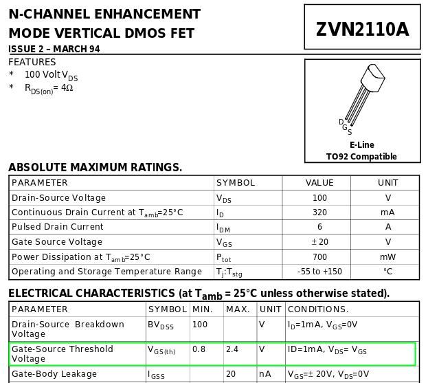
On the breadboard build the circuit from Fig. 23.2 and proceed withe the measurements.

Fig. 23.2 NMOS diode connection diagram
23.2.3. Procedure
Build the circuit from Fig. 23.1 on the breadboard. Set R1=2.2kΩ, R2=10kΩ and R3=1kΩ. For M1 take ZVN211.
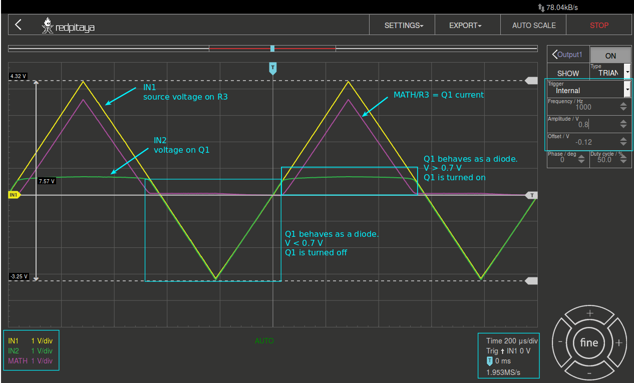
Fig. 23.3 NMOS diode connection on the breadboard
Warning
Before connecting the circuit to the STEMlab -3.3V and +3.3V pins double check your circuit. The -3.3V and +3.3V voltage supply pins do not have short circuit handling and they can be damaged in case of short circuit.
Start the Oscilloscope & Signal generator application
In the OUT1 settings menu set Amplitude value to 0.45V, DC offset to -0.45 V, Frequency to 1kHz to apply the input voltage.
From the waveform menu select TRIANGLE, deselect SHOW and select enable.
On the left bottom of the screen be sure that IN1, IN2 and MATH V/div are set to 1V/div (You can set V/div by selecting the desired channel and using vertical +/- controls).
Set t/div value to 200us/div (You can set t/div using horizontal +/- controls)
Under MATH channel settings set \(IN1-IN2\) and select ENABLE.
Under IN1 and IN2 menu settings set probe to x10 and vertical offset to 0.
Under MATH menu settings set vertical offset to 0.
Under TRIGER settings, set trigger level to 1V

Fig. 23.4 NMOS diode connection measurements
23.2.4. VI curve measurements
Since NMOS can behave as an diode with forward voltage equal to the \(V_{TH}\) (configuration shown on Fig. 23.2) we can measure its VI characteristic as we did when performing diode measurements.For this task we will use Jupyter Notebook Web application. How to start Jupyter Notebook and create new project is shown on figure 5 flow chart.
Note
The Jupyter Notebook is a web application that allows you to create and share documents that contain live code, equations, visualizations and explanatory text. They have also ensured support for the Jupyter application with Red Pitaya libraries enabling control of all features of the STEMlab boards such as: signal acquisition, signal generation, digital signal control, communication etc. The Jupyter Notebook is started on the same way as any other applications. After starting Jupyter application a web based notebook is opened. This combination of the notebook, STEMlab and Python features makes the STEMlab an excellent tool for prototyping and quick programing. Since Jupyter Notebook enables text, equation and picture editing this is a perfect tool for tutorials, examples and ect.
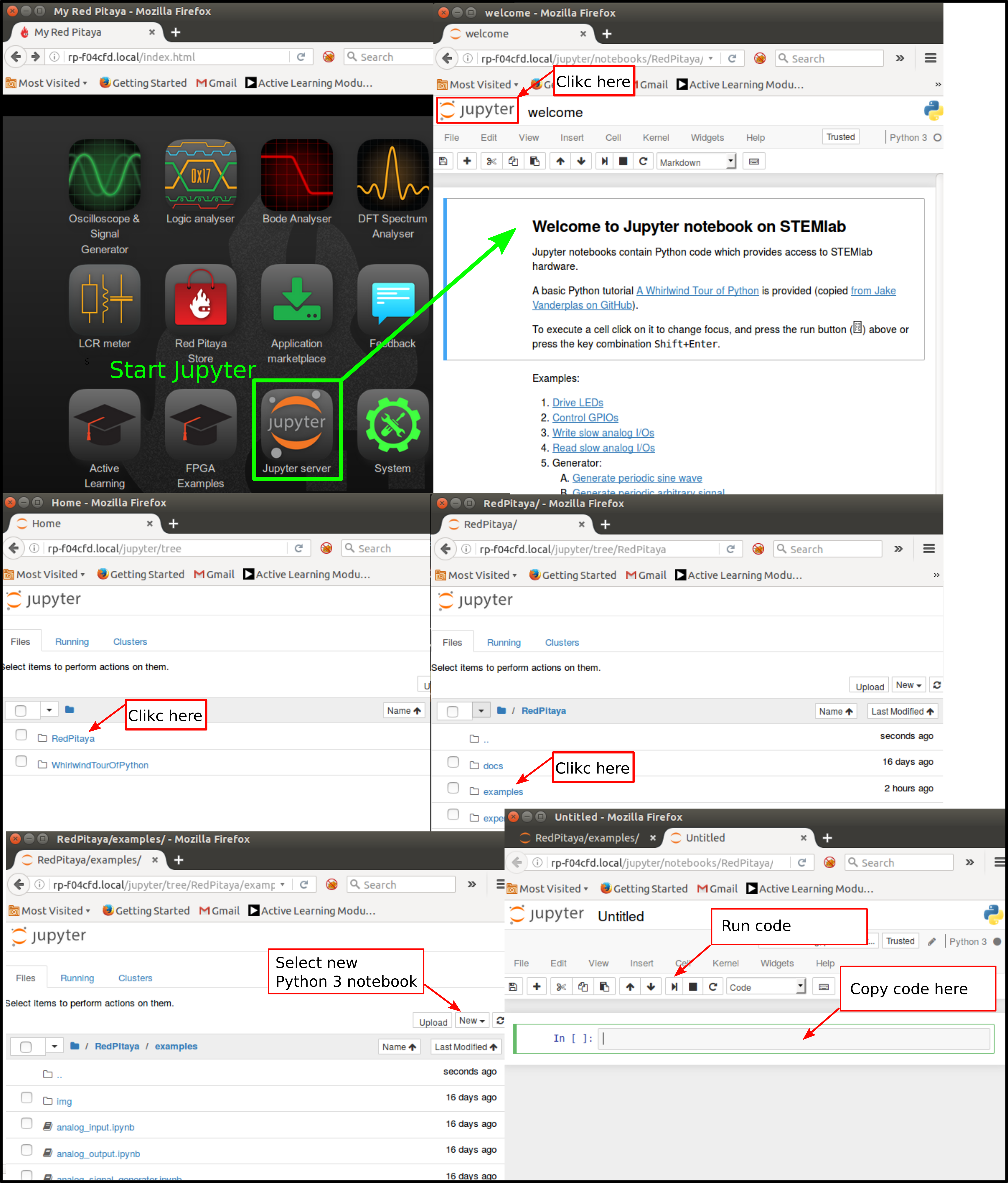
Fig. 23.5 Creating new Jupyter notebook
If you have successfully created new Jupyter notebook then copy-paste code bellow and run it.
Code bellow will generate same signal as from Fig. 23.4 but it will plot them in XY graph.
For measuring \(VI\) curve an “XY” plot is required where x-axis will represent diode voltage \(IN_2\) and y-axis a diode current \((IN_1 - IN_2) / R_3\).
Copy code from below into cell 1
 1# Import libraries
 2from redpitaya.overlay.mercury import mercury as overlay
 3
 4from bokeh.io import push_notebook, show, output_notebook
 5from bokeh.models import HoverTool, Range1d, LinearAxis, LabelSet, Label
 6from bokeh.plotting import figure, output_file, show
 7from bokeh.resources import INLINE
 8output_notebook(resources=INLINE)
 9
10import numpy as np
11
12# Initialize fpga modules
13fpga = overlay()
14gen0 = fpga.gen(0)
15osc = [fpga.osc(ch, 1.0) for ch in range(fpga.MNO)]
16
17# Configure OUT1 generator channel
18gen0.amplitude = 0.45
19gen0.offset = -0.45
20gen0.waveform = gen0.sawtooth(0.5)
21gen0.frequency = 2000
22gen0.start()
23gen0.enable = True
24gen0.trigger()
25
26# R1 resistor value
27R3 = 1000
28
29# Configure IN1 and IN2 oscilloscope input channels
30for ch in osc:
31    ch.filter_bypass = True
32
33    # data rate decimation
34    ch.decimation = 10
35
36    # trigger timing [sample periods]
37    N = ch.buffer_size
38    ch.trigger_pre = 0
39    ch.trigger_post = N
40
41    # osc0 is controlling both channels
42    ch.sync_src = fpga.sync_src["osc0"]
43    ch.trig_src = fpga.trig_src["osc0"]
44
45    # trigger level [V], edge ['neg', 'pos'] and holdoff time [sample periods]
46    ch.level = 0.01
47    ch.edge = 'pos'
48    ch.holdoff = 0
49
50# Initialize diode current and voltage
51V = np.zeros(N)
52I = np.zeros(N)
53
54# Plotting
55hover = HoverTool(mode='vline', tooltips=[("V", "@x"), ("I", "@y")])
56tools = "wheel_zoom, box_zoom, reset,pan"
57p = figure(plot_height=500,
58           plot_width=900,
59           title="XY plot of NMOS transistor VI characteristic",
60           toolbar_location="right",
61           tools=(tools, hover))
62p.xaxis.axis_label = 'Voltage [V]'
63p.yaxis.axis_label = 'Current [mA]'
64r = p.line(V, I, line_width=1, line_alpha=0.7, color="blue")
65
66# get and explicit handle to update the next show cell
67target = show(p, notebook_handle=True)
Create new cell (Insert -> Cell Below) and copy code from below into it.
 1# Measuring I, V and re-plotting
 2while True:
 3    # reset and start
 4    osc[0].reset()
 5    osc[0].start()
 6
 7    # wait for data
 8    while (osc[0].status_run()):
 9        pass
10
11    V0 = osc[0].data(N-100)*10  # IN1 signal
12    V1 = osc[1].data(N-100)*10  # IN2 signal
13    I = ((V0-V1)/R3)*1E3        # 1E3 convert to mA
14    r.data_source.data['x'] = V0
15    r.data_source.data['y'] = I
16    push_notebook(handle=target)
Run Cell 1 and Cell 2. Notice cell 2 is a main loop for the acquisition and re-plotting. If you stop the acquisition just run only cell 2 for starting measurements again.
After running the code above you should get diode VI characteristic as is shown on Fig. 23.6.

Fig. 23.6 NMOS VI characteristic measured using Jupyter Notebook
23.2.5. PMOS as a diode
Same measurements can be also don for PMOS transistor. With PMOS transistor the voltage polarity is reversed so PMOS diode configuration must be different than NMOS one. PMOS diode configuration is shown on Fig. 23.7.

Fig. 23.7 PMOS diode connection diagram
23.2.6. Procedure
Build the circuit from Fig. 23.7 on the breadboard. Set R1=2.2kΩ, R2=10kΩ and R3=1kΩ. For M1 take ZVP211.
Warning
Before connecting the circuit to the STEMlab -3.3V and +3.3V pins double check your circuit. The -3.3V and +3.3V voltage supply pins do not have short circuit handling and they can be damaged in case of short circuit.
Start the Oscilloscope & Signal generator application.
In the OUT1 settings menu set Amplitude value to 0.45V, DC offset to -0.45 V, Frequency to 1kHz to apply the input voltage.
From the waveform menu select TRIANGLE, deselect SHOW and select enable.
On the left bottom of the screen be sure that IN1, IN2 and MATH V/div are set to 1V/div (You can set V/div by selecting the desired channel and using vertical +/- controls)
Set t/div value to 200us/div (You can set t/div using horizontal +/- controls)
Under MATH channel settings set \(IN1-IN2\) and select ENABLE.
Under IN1 and IN2 menu settings set probe to x10 and vertical offset to 0.
Under MATH menu settings set vertical offset to 0.
Under TRIGER settings, set trigger level to 1V
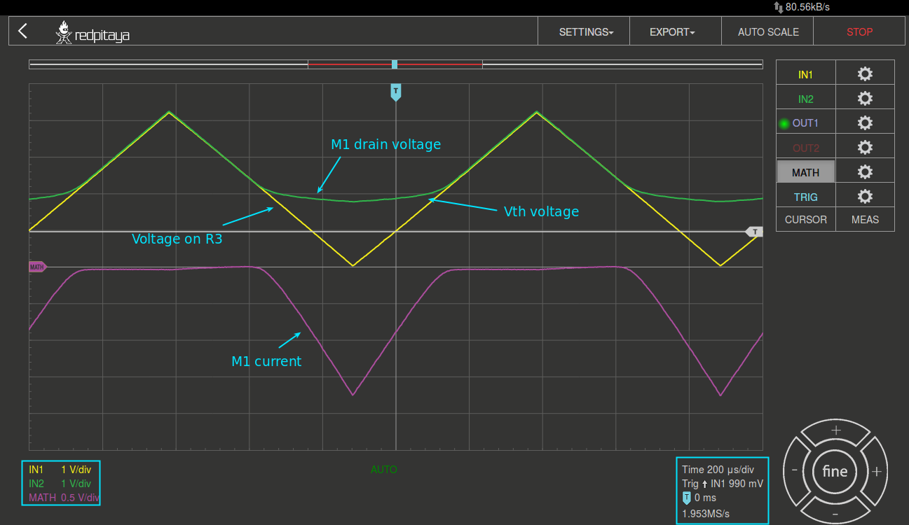
Fig. 23.8 PMOS diode connection measurements
As we can see from Fig. 23.8 the PMOS in diode configuration behaves as an diode with forward drop voltage equal to the PMOS \(V_{TH}\).
Compare Fig. 23.8 and Fig. 23.4 and try to explain the difference between NMOS and PMOS diode configurations.