17. Current Sensing using a Difference Amplifier
17.1. Objective
The objective of this lab activity is to investigate current sensing techniques that use an op-amp configured as a difference amplifier.
17.2. Notes
In this tutorials we use the terminology taken from the user manual when referring to the connections to the Red Pitaya STEMlab board hardware. Extension connector pins used for -3.3V and +3.3V voltage supply are show in the documentation here. Oscilloscope & Signal generator application is used for generating and observing signals on the circuit.
17.3. Background
We have investigated the difference amplifier. Now we will use it as a current sense amplifier. One of the major applications of the op-amp difference amplifier is in measuring the current at point in a circuit other than where it flows into or out of ground or the common node. The current to be measured is converted into a small voltage by breaking open the current path and inserting a low value resistor in series. This resistor is called a current shunt resistor or just shunt. The resistance is kept small and the voltage drop across the shunt small to reduce any effect this change might have on the operation of the circuit. Current going through shunt resistor therefore path current is given as
Since differential voltage across resistor (given as \(\Delta V = V_{R_{shunt_{node_1}}}-V_{R_{shunt_{node_2}}})\) should be measured we can see that a difference amplifier is an ideal circuit for that task. The small differential voltage drop across the shunt is amplified and converted to a single ended (common referenced) voltage by an op-amp difference amplifier.
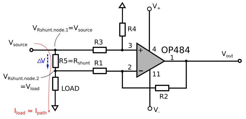
Figure 1: Basic Difference Amplifier in current sensing configuration
From the figure 1 we know that differential voltage \(\Delta V\) given as \(\Delta V = I_L R_s\) is carrying information about LOAD current. Also from difference amplifier theory we know that \(\Delta V\) will be somehow related to the \(V_{out}\). First assumption is as following:
or,
In other words; simply by measuring and scaling \(V_{out}\) we will measure load current, where \(R_{s}\) is shunnt resistor. Transfer characteristic of difference amplifier for circuit shown on figure 1 is:
Where \(V_{+}\) and \(V_{-}\) are voltages on noninverting(pin 3) and inverting(pin 2) opamp inputs respectively. Substituting \(V_{+}\) and \(V_{-}\) for voltages on shunt resistor nodes we get
where \(V_S\) is source voltage and \(V_L\) load voltage. We can also write
and
On the first look, by adding resistor \(R_4\) to the circuit, shown on figure 1, somehow we have complicated transfer function; from equation (2) to equation (3). But adding \(R_4\) is necessary in order to equalize factor \(1+R_2/R_1\) to the factor \(R_2/R_1\) from the equation (2) in order to get opamp input voltages equally amplified and therefore enabling simple \(\Delta V\) to \(V_{out}\) correlation. The important step is to select values of \(R_3\) and \(R_4\) as
Using identities above we can write equation (3) as
It holds that
So we can write equation (4) simple as:
Now we have simple equation (5) for our difference amplifier form figure 1 and the last step is to rewrite it in terms of \(\Delta V\) i.e in terms of \(I_L\)
Note
And for \(I_L\) we get:
17.3.1. In our example we have
Note
In our example load current is given as
\[I_L = \frac{V_{out}}{100} \quad (8)\]
17.4. Materials
Red Pitaya STEMlab
OPAMP: 1x OP484 quad rail to rail amplifier
Resistor: 3x 10 \(k \Omega\)
Resistor: 1x 100 \(k \Omega\)
Resistor: 1x 10 \(\Omega\)
Resistor: 1x 220 \(\Omega\)
Capacitor: 1x 0.1 \(\mu F\)
Inductor: 1x 4.7 \(mH\)
17.5. Directions
Build the current sense amplifier shown in figure 2. R6 is added to stabilize the output of the OP484. When using large feedback resistances the OP484 can be unstable due to the large input capacitance of the IN2 input. \(V_{S}\) is provided directly from the OUT1 STEMlab output as “power supply” for the LOAD. The load will consist of different impedances such as a resistor, capacitor or inductor. IN2 input voltage signal will directly show load current as is shown in the equation 8.
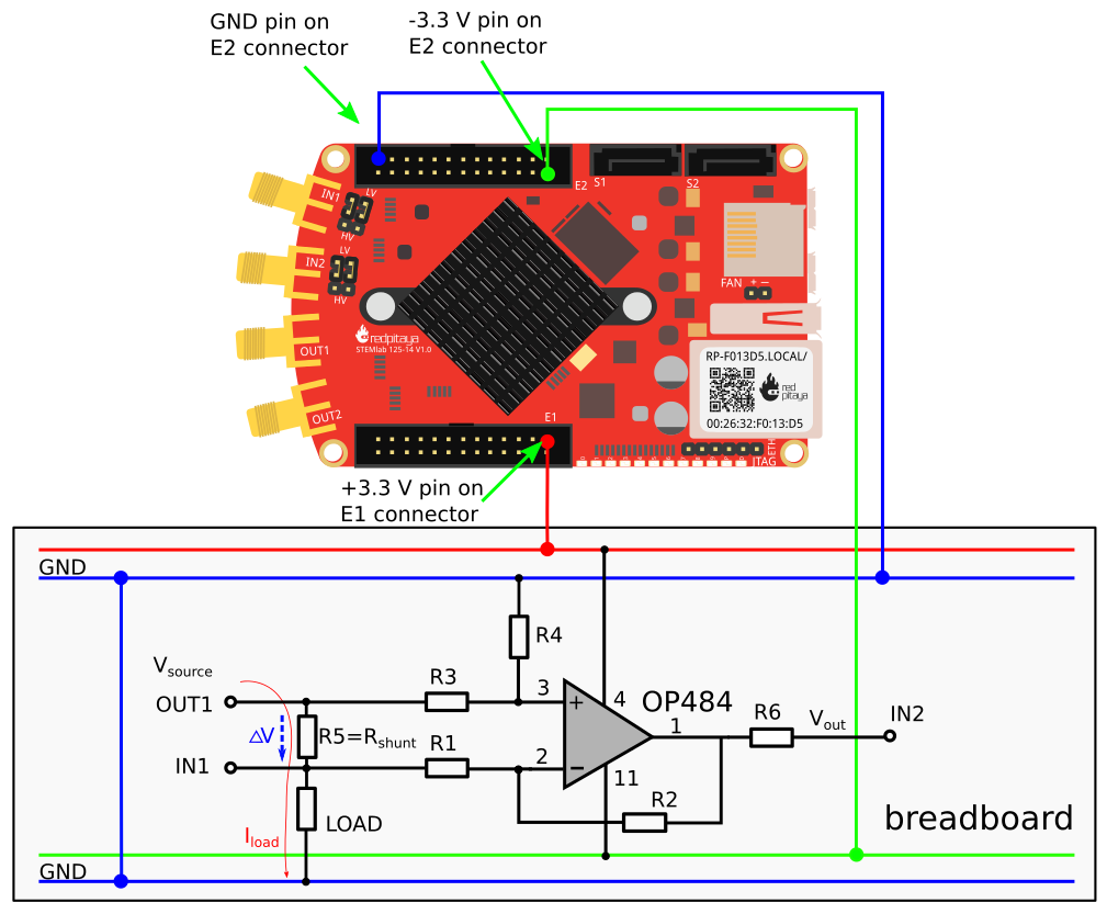
Figure 2: Difference Amplifier circuit for current sensing
Components values are next:
17.6. Procedure
17.6.1. Resistor LOAD
For LOAD take \(470 \Omega\) resistor and build circuit shown on figure 2.
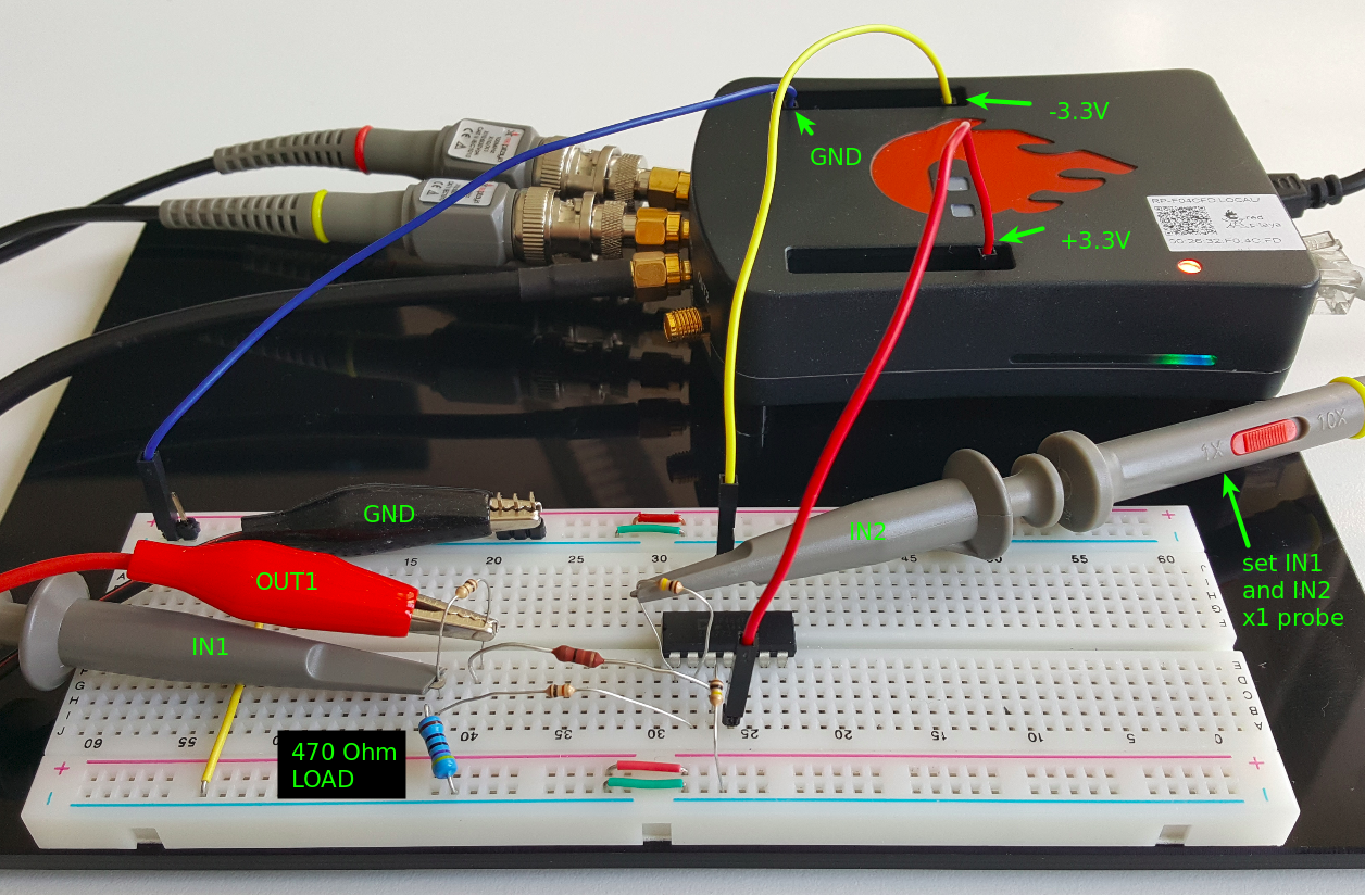
Figure 3: Difference Amplifier circuit for current sensing - Resistive LOAD
Start the Oscilloscope & Signal Generator application.
In the OUT1 settings menu set Amplitude value to 0.5V to apply a sine wave as the input voltage \(V_{source}\). From the waveform menu select SINE, deselect SHOW button and select enable.
For the stable acquisition set the trigger source to IN1
On the left bottom of the screen be sure that IN1 V/div is set to 200mV/div (You can set V/div by selecting the desired channel and using vertical +/- controls)
On the left bottom of the screen be sure that IN2 V/div is set to 50mV/div (You can set V/div by selecting the desired channel and using vertical +/- controls)
In the measurement menu select “MAX” , select IN1 and press DONE
In the measurement menu select “MAX” , select IN2 and press DONE
Set t/div value to 200us/div (You can set t/div using horizontal +/- controls)
Readout measurements of IN2 and calculate load current using equation (8)
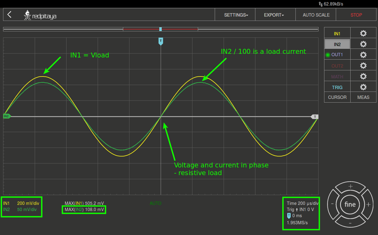
Figure 4: Resistive LOAD current measurements
From the measurements from figure 4 we can calculate max load current as:
We can check our measurements by calculating load current as
We can see that measured current is as what we expected confirming correct behaviour of our difference amplifier. The difference of 0.04mA between exact and measured value of load current comes from nominal tolerances values of load and shunt resistors.
17.6.2. Capacitance LOAD
For LOAD take \(0.1 \mu F\) capacitor and build circuit shown on figure 2.
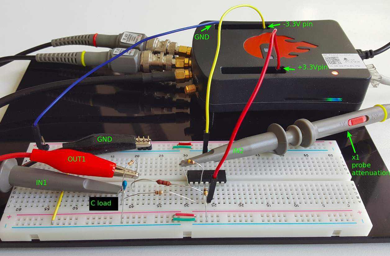
Figure 5: Capacitance LOAD
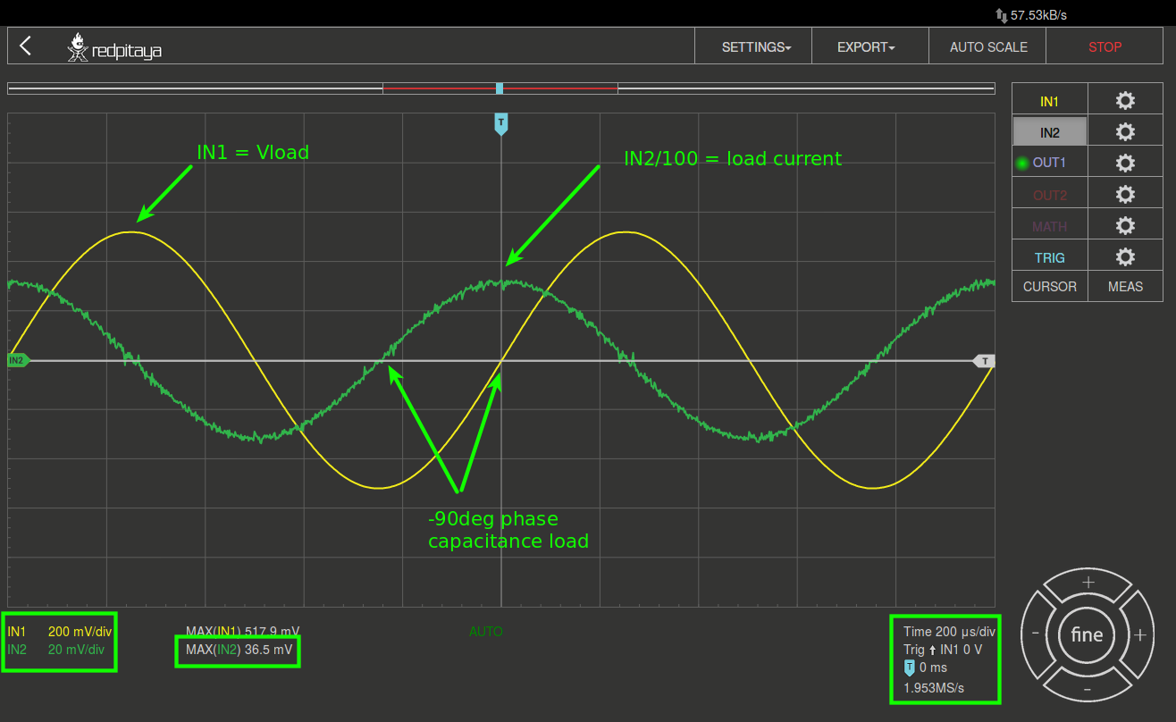
Figure 6: Capacitance LOAD current measurements
From the measurements from figure 6 we can calculate max load current as:
We can check our measurements by calculating load current as
17.6.3. Inductive LOAD
For LOAD take \(4.7 mH\) inductor and build circuit shown on figure 2.
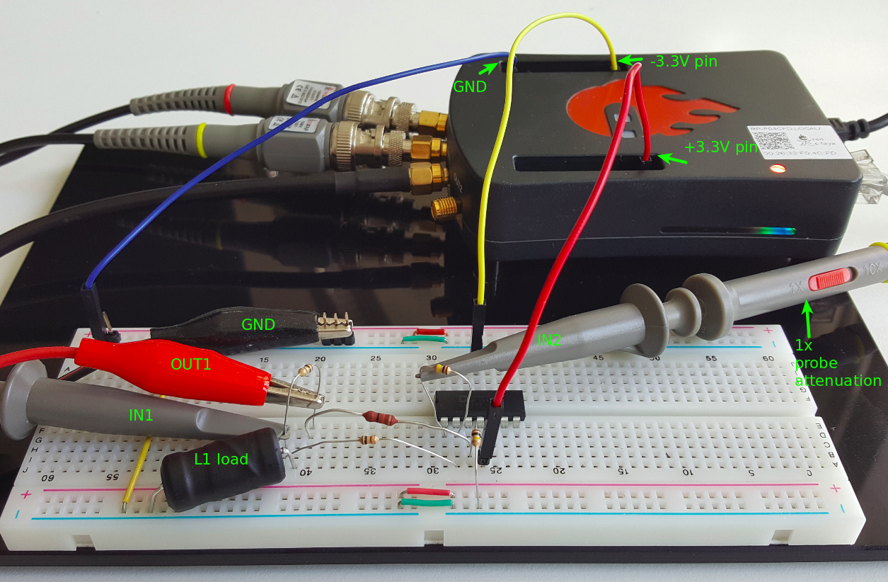
Figure 7: Inductive LOAD
In the OUT1 settings menu set Amplitude value to 0.2V
On the left bottom of the screen be sure that IN1 V/div is set to 50mV/div (You can set V/div by selecting the desired channel and using vertical +/- controls)
On the left bottom of the screen be sure that IN2 V/div is set to 500mV/div (You can set V/div by selecting the desired channel and using vertical +/- controls)
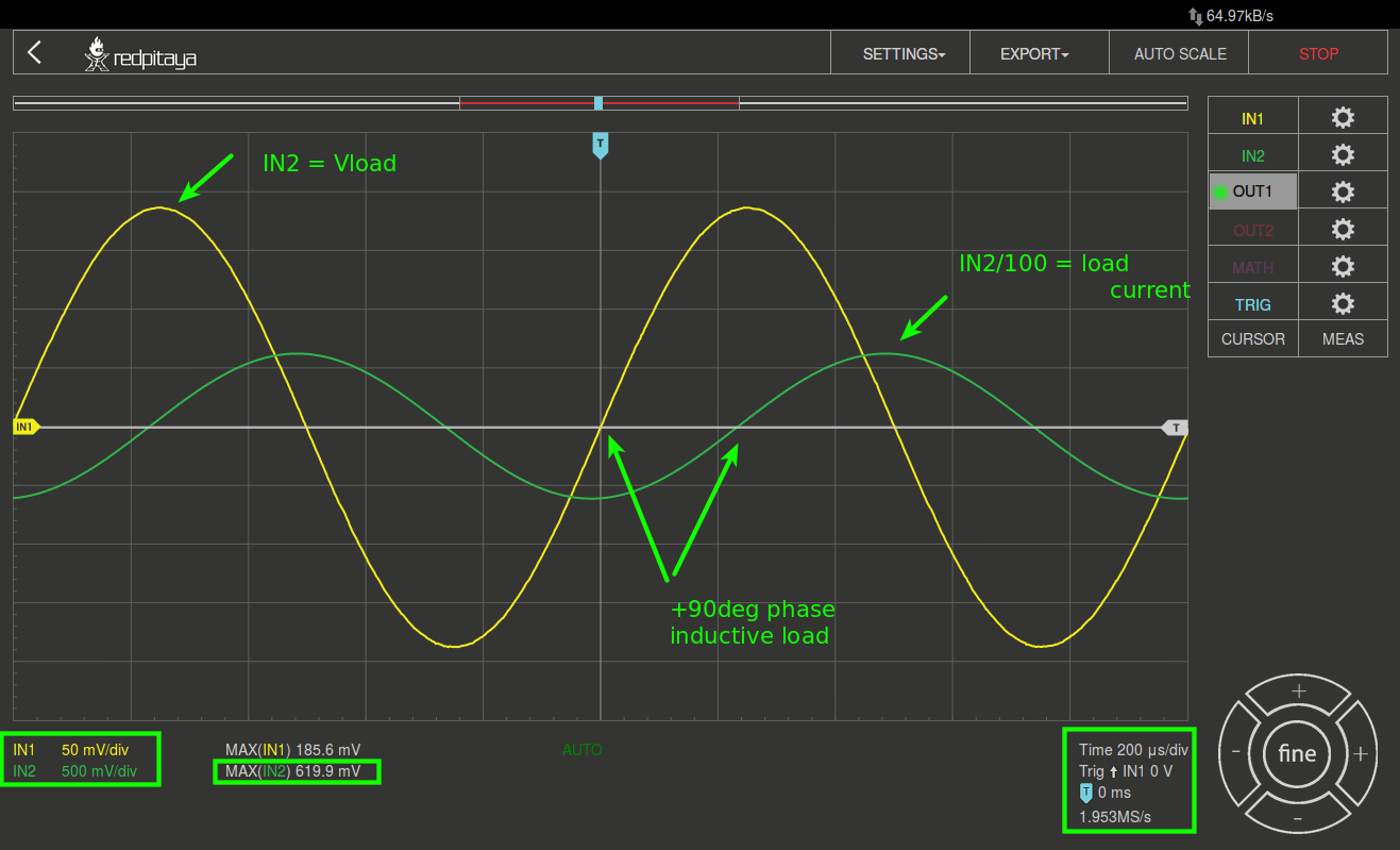
Figure 8: Inductive LOAD current measurements
From the measurements from figure 8 we can calculate max load current as:
We can check our measurements by calculating load current as
Note
At inductive load we have largest difference in measurements. Try to explain why. Hint. parasitics, series resistance of an inductor.